


Introduction
An FPGA is a semiconductor chip that loads configuration data into internal cells. The configuration data determines which gates will have an input and open (a sequence). FPGAs are used in designs that need flexibility and can’t be fixed in a circuit fabrication (e.g., web servers). Most of them have add-in-card connectors that allow them to be integrated with a system. This allows a single design to be built from numerous FPGA chips. They can also be programmed in systems that already have an ASIC, such as a DSP or CPU.
The flexibility, efficiency, and cost of an FPGA make it an ideal hardware accelerator for high-volume products as diverse as telecom system base stations, computer graphics accelerators, radio communications/wireless infrastructure systems, medical equipment, and aerospace instrumentation. A Xilinx FPGA offers products that address the needs of embedded designers on many levels. These include:
Embedded FPGA: Xilinx’s standard embedded FPGA is a development platform used to design a wide variety of embedded systems with minimal engineering time. Xilinx’s products provide a complete software development environment (SDK), pre-verified, high-quality modules, and other resources for rapid system design and prototyping, as well as automated test support for hardware/software verification and validation.
Types of FPGAs 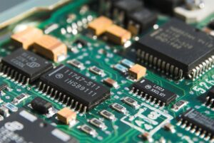
An FPGA may be classified by the configuration data they accept, either as a “programmable logic device” (PLD), “configurable logic device” (CLD), or both types.
FPGAs based on a PLD or CLD can be classified as programmable fabric, reprogrammable fabric, or reconfigurable fabric, depending on whether extra configuration data has to be loaded with the fabrication process.
A PLD is functionally equivalent to an ASIC, and its pins are permanently assigned to gates. The configuration data is stored as a bit file on an external memory device, such as flash memory or static RAM.
A CLD contains a circuit built up of flip-flops that form the basic logic gate building blocks. The CLD’s configuration data is a netlist written in HDL (hardware description language). The hardware designer uses tools to convert the design into logic gates and assign particular resources to the underlying hardware platform. The FPGA’s design can be thought of as an algorithm. The algorithm is represented as a sequence of logic gates, input pins, and output pins.
Functions of an FPGA
- Add/delete user-specified functions
- High performance for time-sensitive applications
- High density, small footprint, and low power consumption
- Hardware Reconfigurable Customization of the FPGA module.
- Hardware acceleration of the DSP.
They are, however, used in several products and applications, including network processor set-top boxes, graphics accelerators, high-performance processing systems, and ASICs.
Advantages of an FPGA 
They can be programmed with configuration data as part of the process. Since programming an ASIC is time-consuming and expensive, most designs are hand-waved. This leaves minimal alteration, other than a few tweaks in the design and calling for a new board layout.
Because of their great flexibility, designers can use them for various applications. They have been used in numerous projects, including computer graphics accelerators and network processors. It has a primary circuit for a more extensive system consisting of standard base modules and add-ons. Also, they are more fruitful in their applications as they are designed to be re-programmed with a specific task, rather than being made for only one program.
Best Server hosting for Minecraft Gaming


